


 9 / 12

9
INNOVATIONEN
F
orschung,
Innovation
und Produkte, die kon-
sequent für die Bedürf-
nisse und die Anforde-
rungen der Kunden entwickelt
wurden und darauf abgestimmt
sind – das sind die Elemente,
aus denen intelligente Lösungen
gemacht sind.
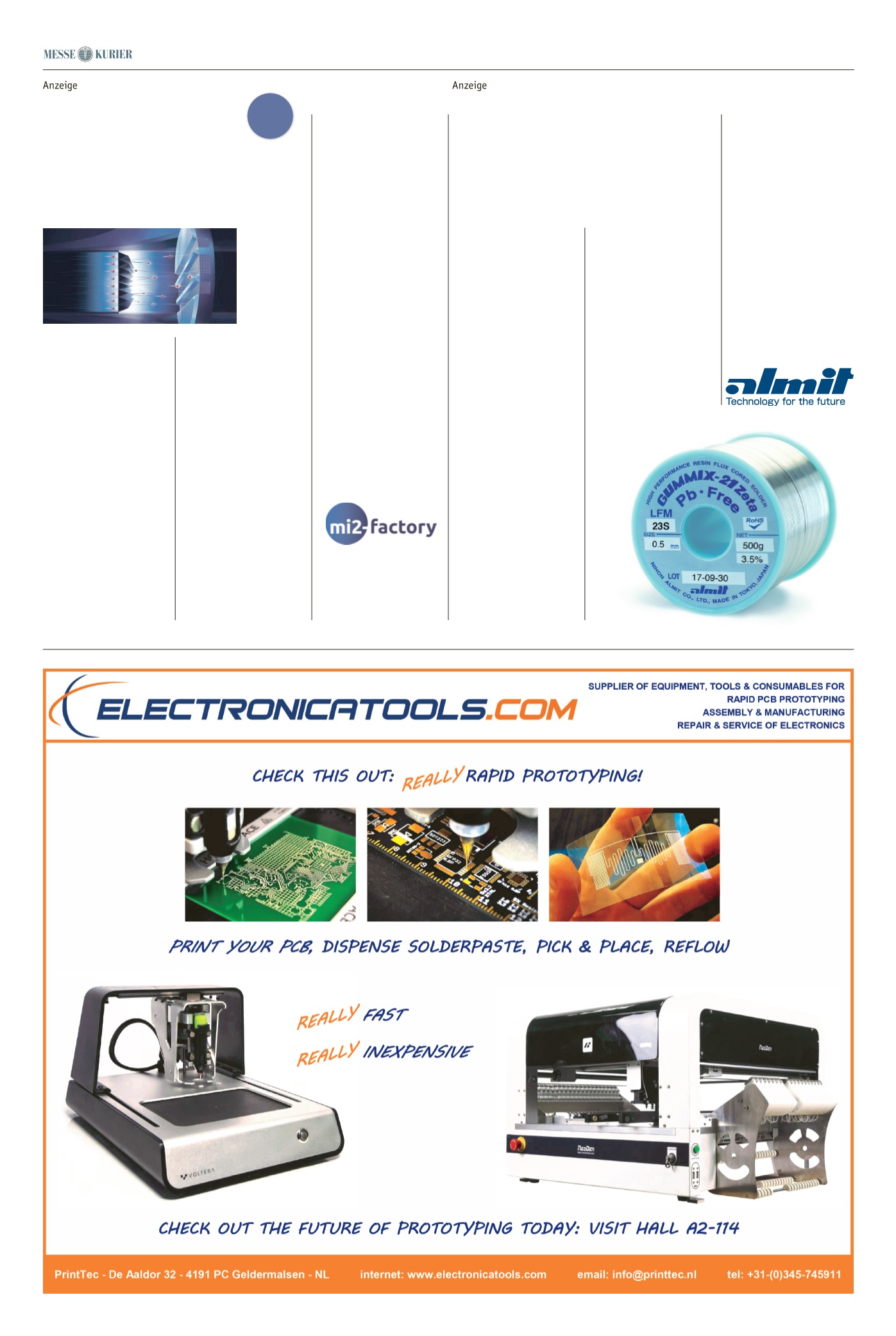
Die Almit GmbH aus Michelstadt
steht mit ihren innovativen Löt-
drähten, Lötpasten und Flussmit-
teln genau für diese intelligenten
Lösungen. In den Forschungslabo-
ren und Technologiezentren von
Nihon Almit in Japan und in an-
deren Ländern forschen jeden Tag
zahlreiche Mitarbeiter nach neuen
Wegen und entwickeln bisher un-
bekannte Möglichkeiten, Lötpro-
zesse weiter zu perfektionieren.
Ein hervorragendes Beispiel für
intelligente Lösungen ist das neue
LFM-23 S von Almit – eine SnCuNi-
Legierung mit einer innovativen
Eisen-/Gallium- Verbindung, die
eine bis zu 5-fach längere Löt-
spitzenstandzeit garantiert. Die
Lötspitze muss weniger häufig ge-
wechselt werden und trägt so dazu
bei, die Kosten in der Produktion
deutlich zu reduzieren.
Es ist aber nicht nur die Kos-
tenreduktion allein, die LFM-23
S zu einer intelligenten Lö-
sung macht: Durch die längere
Verwendbarkeit der Lötspitze
wird auch weniger Material ver-
braucht und somit die Nach-
haltigkeit und der bewusste
Umgang mit Rohstoffen unter-
stützt.
Ein weiteres Beispiel für intel-
ligente Lösungen aus dem Hoch-
leistungs- Sortiment von Almit
ist die bekannte und hundert-
tausendfach bewährte und pa-
tentierte Legierung SJM (Strong
Joint Metal). SJM garantiert,
obwohl bleifrei und niedrig-
silberhaltig, eine überragende
Performance bei der Lötstellen-
Festigkeit.
Welche der intelligenten Lö-
sungen von Almit die richtige
ist, um Ihrer Produktion neue
Möglichkeiten und Chancen zu
eröffnen, erfahren Sie am besten
bei einem Besuch am Stand von
Almit in Halle A4, Stand 435.
Das Hochleistungssortiment von
Almit bietet für jede Aufgabe
und Anforderung die individuell
perfekte Lösung.
T
he mi2-factory is a Ger-
man high-tech SME with
focus on semiconductor
wafer processing. mi2-
factory has developed a novel
semiconductor doping process,
based on the proprietary, micro-
engineered energy filter for high-
energy ion implantation (EFII).
EFII enables very precise, deep.
custom-designed, depth-distribut-
ed doping profiles in any desired
semiconductor material. Custom-
ers engaged in SiC production in
particular do benefit from this
unique, high-throughput, low-cost
doping approach.
You look for an attractive in-
vestment opportunity? Come and
make your invest in our company
to secure your participation in a
highly promising, future-orientat-
ed technology! You will partici-
pate in the booming silicon car-
bide market and
you will profit
from the key role
of mi2-factory.
M i c r o e l e c -
tronic
power
devices based
on the semicon-
ductor material
silicon carbide (SiC) have superior
properties compared to devices
made of Silicon (Si). One of the key
processes during the production of
any SiC power device is the dop-
ing of the active epitaxial layer.
Unfortunately, today’s microchip
production cannot fully exploit
the advantages of SiC, since the
doping variance of the active layer
is rather high (more than 10%
doping variation for N (nitrogen)
in SiC across a 6” wafer is com-
mon). This directly translates into
negative device performance and
higher chip cost. Until recently, no
technical solutions to overcome
this problem were known, that are
scalable to production volume.
The EFII technology overcomes
the above mentioned problems in
semiconductor doping in a scal-
able manner. It especially offers
a highly-precise, flexible solution
for the doping problem in SiC;
less than 3% doping variation for
N (nitrogen) in SiC across a 6” wa-
fer can be achieved. The technolo-
gy is based on the transmission of
accelerated ions through a micro-
patterned, thin silicon membrane,
which is referred to as EFII. The
EFII manipulates the energy dis-
tribution of the formerly monoen-
ergetic ion beam into a continuous
energy distribution, allowing for
depth distributed, highly precise
and (if needed) masked doping.
The EFII technology is offered to
semiconductor power device man-
ufacturers which are in particular,
but not exclusively dealing with
silicon carbide (SiC) high-voltage
diodes, MOSFETs (metal oxide sem-
iconductor field-effect transistors)
and superjunction devices and also
to SiC substrate suppliers. Further-
more EFII is offered to high-ener-
gy ion implantation foundries, ion
beam accelerator manufacturers
and end-station manufacturers.
For all target groups technical co-
operation agreements and/or com-
mercial agreements with technical
assistance are envisaged.
Visit us between 14.-17.11.2017 on Semicon Fair at booth B1-1040 or in the Internet at www.mi2-factory.com!Halle A4, Stand 435
Intelligente Lösungen
haben viele Vorteile
mi2-factory GmbH
Your Industry Partner
or Investment Project
Hall B1
Stand 1040